Hardware
Hardware Requirements
Using every firmware feature requires the hardware belonging to the BSC system. Detailed hardware documentation, including the circuit diagram, is in the hardware repository.
We currently recommend LILYGO T-CONNECT. The original BSC mainboard is no longer regularly available and is no longer a recommended purchasing option. See Obtaining Hardware.
An ESP32 development kit can be used for initial testing, but some functions are restricted or untested. See Testing Without Original Hardware.
LILYGO T-CONNECT
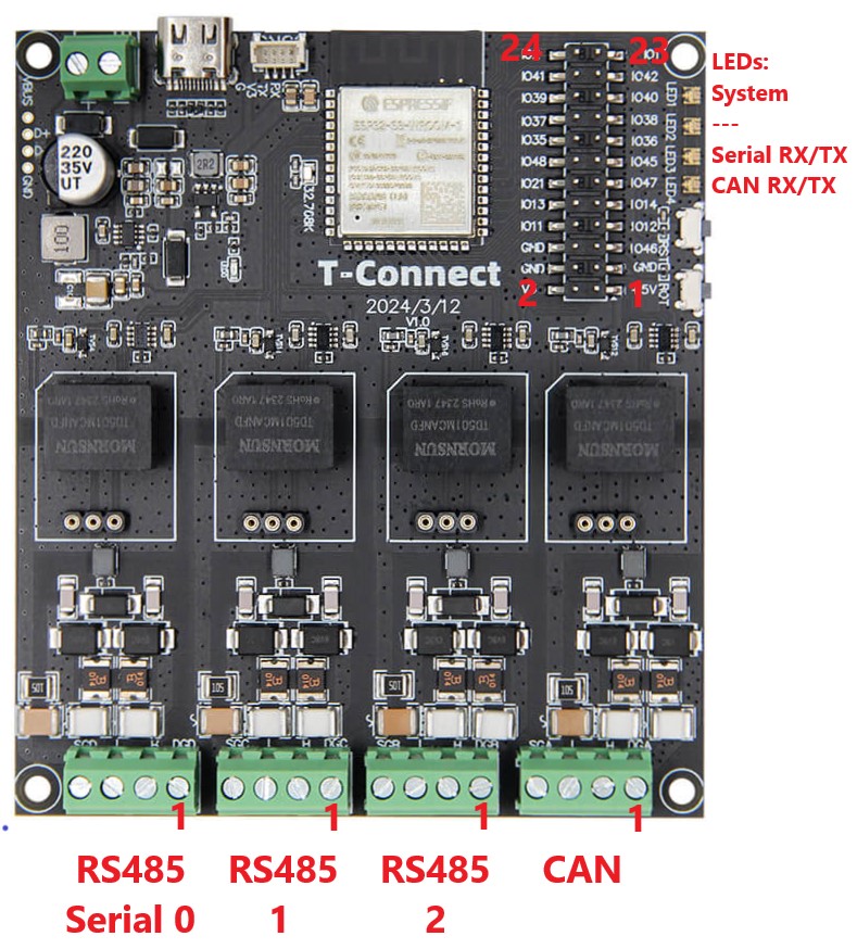
Connector Pinout
| Pin | Serial 0–2 (RS485) | CAN |
|---|---|---|
| 1 | --- | --- |
| 2 | B | H |
| 3 | A | L |
| 4 | GND | GND |
LED Functions
| LED | Colour | Function |
|---|---|---|
| System | Blue | System is booting |
| System | Flashing green | System is operating without errors |
| System | Flashing red | One of the system tasks is not responding |
| Serial RX/TX | Flashing red | Communication with a BMS |
| CAN RX/TX | Flashing red | Sending a CAN message |
Pin Header Assignment
The documented firmware provides OneWire and I²C (for example for the display) on the pin header.
| Pin | GPIO | Standard | W5500 | MCP2518 |
|---|---|---|---|---|
| 1 | 5 V | 5 V | 5 V | |
| 2 | 3.3 V | 3.3 V | 3.3 V | |
| 3 | GND | GND | GND | |
| 4 | GND | GND | GND | |
| 5 | 46 | INT | ||
| 6 | GND | GND | GND | |
| 7 | 12 | I²C SCL | SPI SCK | |
| 8 | 11 | I²C SDA | SPI MOSI | |
| 9 | 14 | SE RX | SE RX (without W5500 only) | |
| 10 | 13 | SE TX | SPI MISO | SE TX (without W5500 only) |
| 11 | 47 | SPI MISO | ||
| 12 | 21 | INT | ||
| 13 | 45 | SPI SCK | ||
| 14 | 48 | SPI MOSI | ||
| 15 | 36 | |||
| 16 | 35 | |||
| 17 | 38 | OneWire | OneWire | OneWire |
| 18 | 37 | |||
| 19 | 40 | |||
| 20 | 39 | I²C SDA | ||
| 21 | 42 | |||
| 22 | 41 | I²C SCL | ||
| 23 | 1 | CS | ||
| 24 | 2 | CS | ||
| – | 43 | SE TX | ||
| – | 44 | SE RX |
The firmware documented for this version provides OneWire, relay outputs, digital inputs and I²C (for example for the display) on the pin header.
| Pin | GPIO | Function |
|---|---|---|
| 1 | 5 V | |
| 2 | 3.3 V | |
| 3 | GND | |
| 4 | GND | |
| 5 | 46 | --- |
| 6 | GND | |
| 7 | 12 | I²C SCL |
| 8 | 11 | I²C SDA |
| 9 | 14 | SE RX |
| 10 | 13 | SE TX |
| 11 | 47 | --- |
| 12 | 21 | OneWire |
| 13 | 45 | --- |
| 14 | 48 | --- |
| 15 | 36 | Digital input 1 |
| 16 | 35 | Digital input 2 |
| 17 | 38 | Digital input 3 |
| 18 | 37 | Digital input 4 |
| 19 | 40 | Relay 1 |
| 20 | 39 | Relay 2 |
| 21 | 42 | Relay 3 |
| 22 | 41 | Relay 4 |
| 23 | 1 | Relay 5 |
| 24 | 2 | Relay 6 |
BSC Display
The display and its firmware are maintained in a separate project.
Supported Display
We have tested display hardware version 3.3. The display is available from the BSC Shop.
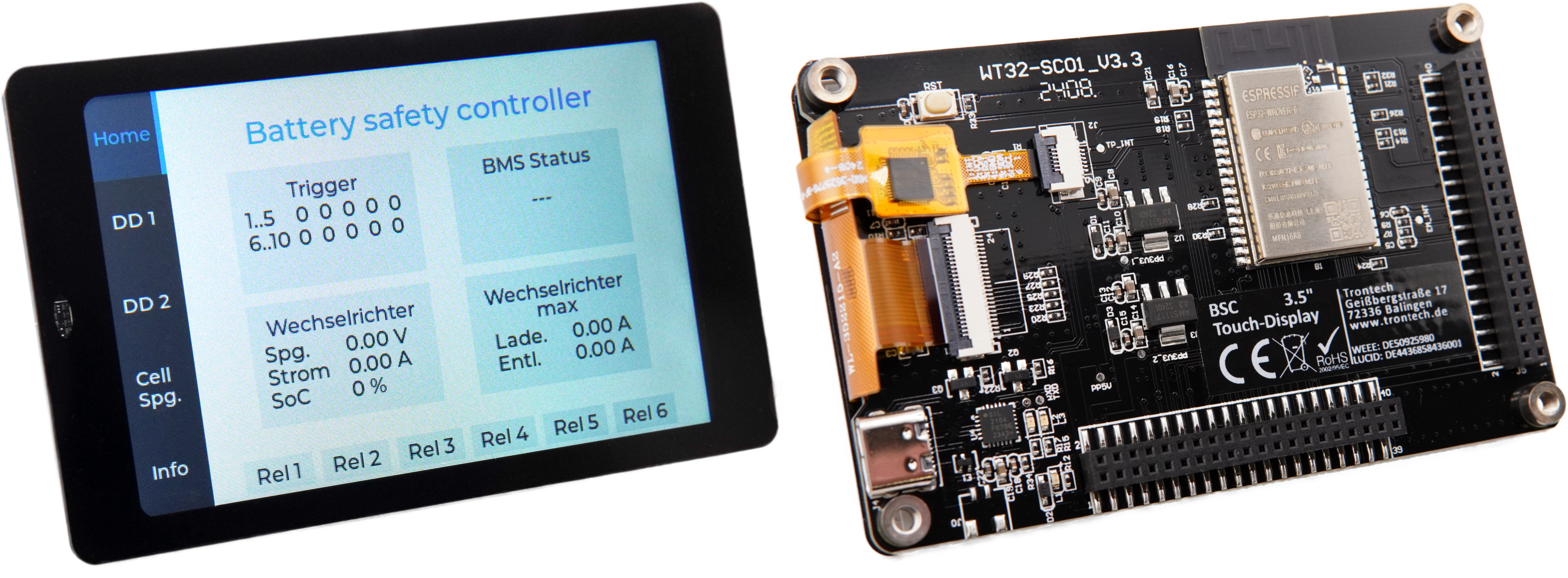
Connecting to the BSC Mainboard
Recommended: Mainboard-Display Connection Kit
For tool-free assembly without soldering or wiring mistakes, we recommend the Mainboard-Display Connection Kit. It contains two adapter boards and a ribbon cable.
- No manual soldering.
- Tool-free plug-in assembly.
- Mechanically keyed connections help prevent wiring errors.
- Status LED for function checking.
- Compatible with every mainboard revision.
Alternative: Manual Connection
Connect manually through extension port J3: the I²C data connection uses SCL/SDA, and the port's 5 V and GND can power the display.
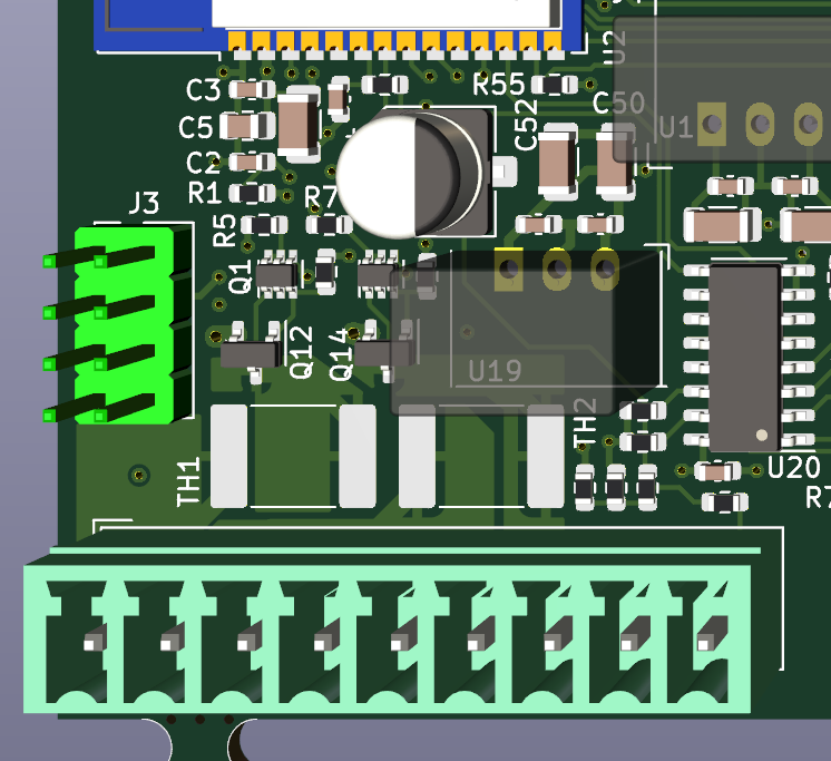
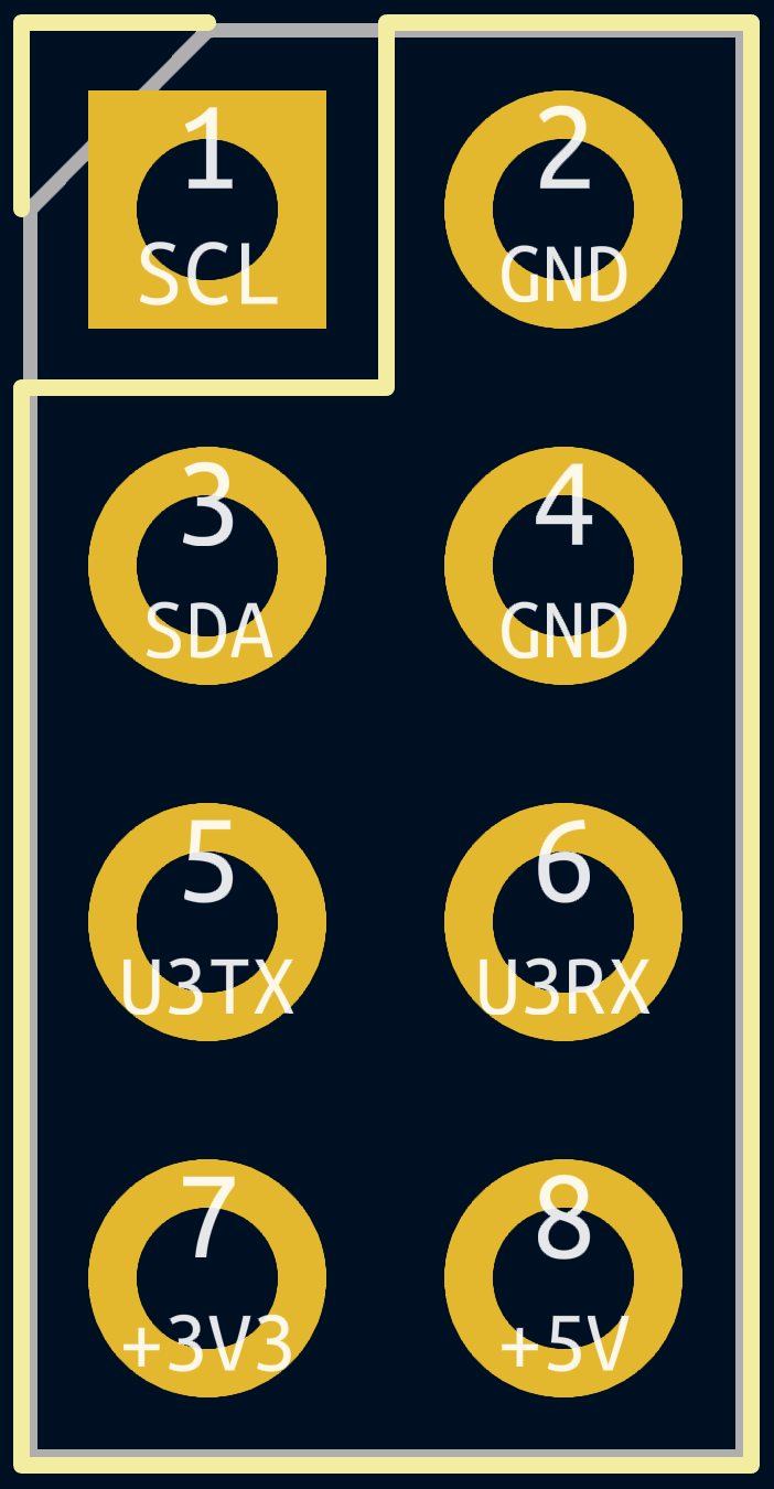
WT32-SC01 Display Pinout
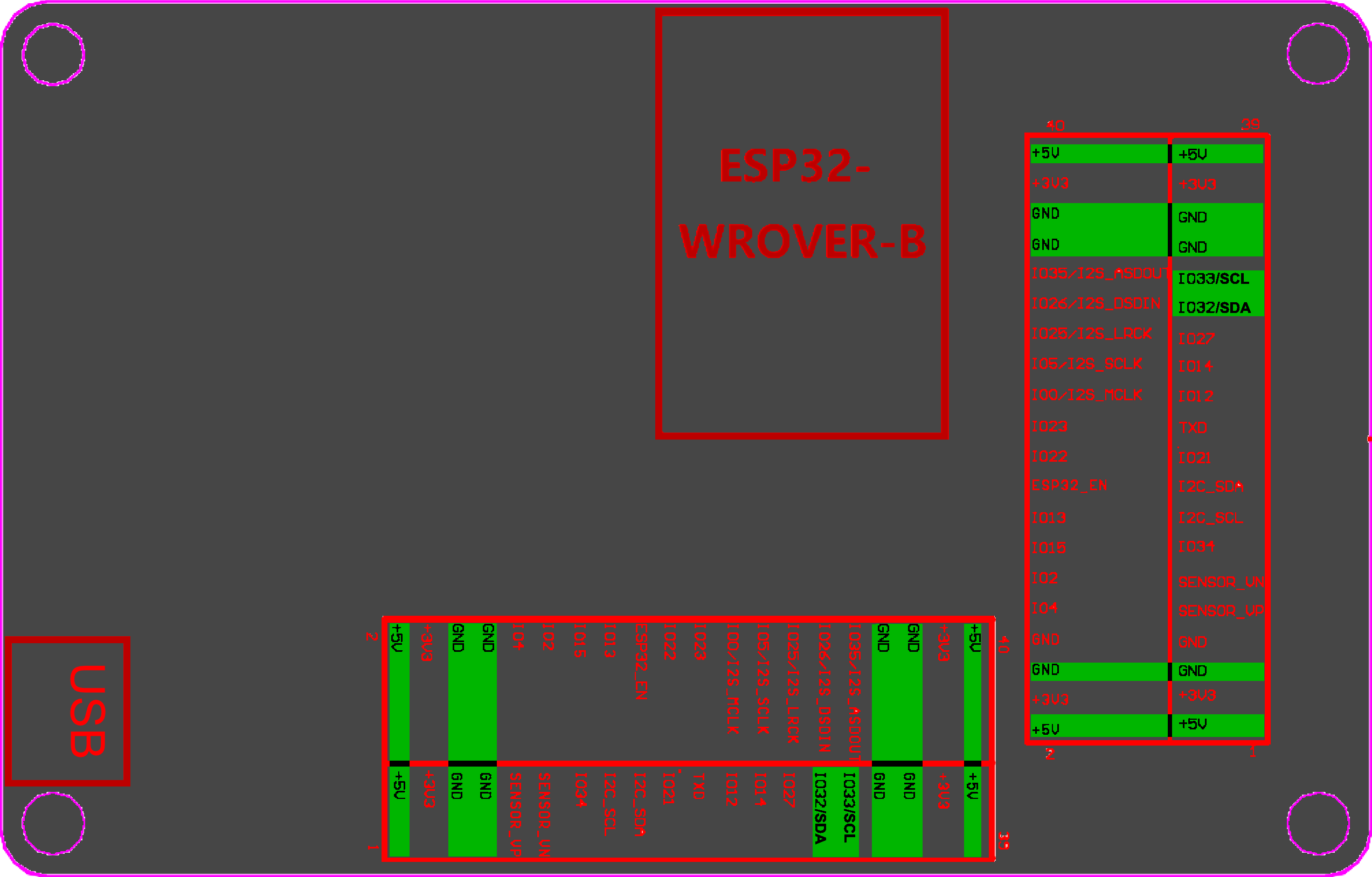
Original BSC Mainboard
Availability
The original BSC mainboard is no longer regularly available. Use LILYGO T-CONNECT for new installations instead.
Handling Connections
A technical talk about connections is available on YouTube.
Connecting Screw Terminals Correctly
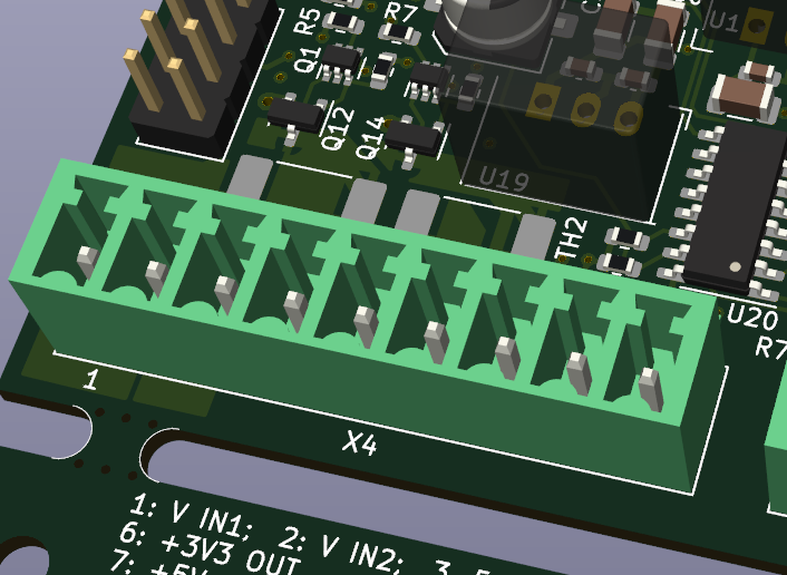
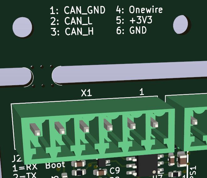
- Pin 1 marking: Each screw terminal has a
1identifying its first pin. Use it as your connection reference. - Function labels: Read the function labels beside the pin-1 marking carefully before connecting wires.
- Safety: Incorrect connections can damage the BSC or connected components.
- Illustrations: Images in this documentation are illustrative only. Always verify the markings and labels on your own PCB.
Power Supply
The PCB labels identify V IN1 as positive and GND as negative. The standard BSC hardware is designed for 5 V (>= 1.5 A). Meanwell DIN-rail supplies, available from the BSC Shop, have proven reliable.
Use a redundant supply so that a second supply takes over without interruption if the first fails. For example, connect a battery-powered DC/DC supply and a grid-powered AC/DC supply to the two separate inputs. Set the preferred primary source about 0.2 V higher; the supply with the higher voltage powers the BSC.
Increasing the Supply Voltage
Supply voltages above 5 V, such as 12 V or 24 V, are possible under these conditions. PCB reference designators changed between revisions; the pairs below mean HwRev < 2.5 / HwRev >= 2.5.
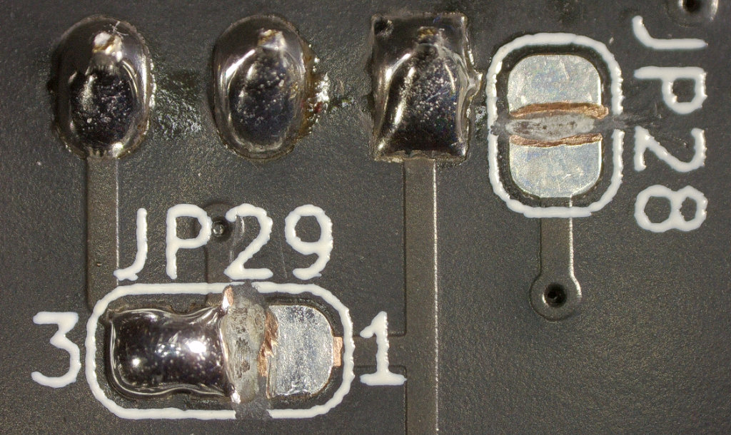
- JP28 / R61 (BSC component supply): Normally bridged; open this connection for supply voltages above 5 V. It is labelled on the PCB underside, beside U19's solder connections.
- JP29 / R91 and JP25 (relay supply): No changes are needed for 5 V relays. If JP25 connects relay COM contacts to the supply, use no more than 24 V. To power higher-voltage relays above 5 V without loading U19:
- HwRev < 2.5: open connection 2–1 and solder-bridge 3–2. On BSC V2.3, JP29 is mislabelled: pin 1 is on the right, although the print places it on the left.
- HwRev >= 2.5: remove R91 and close solder jumper JP25.
- Above 19 V, reversed polarity can damage components. Check polarity explicitly.
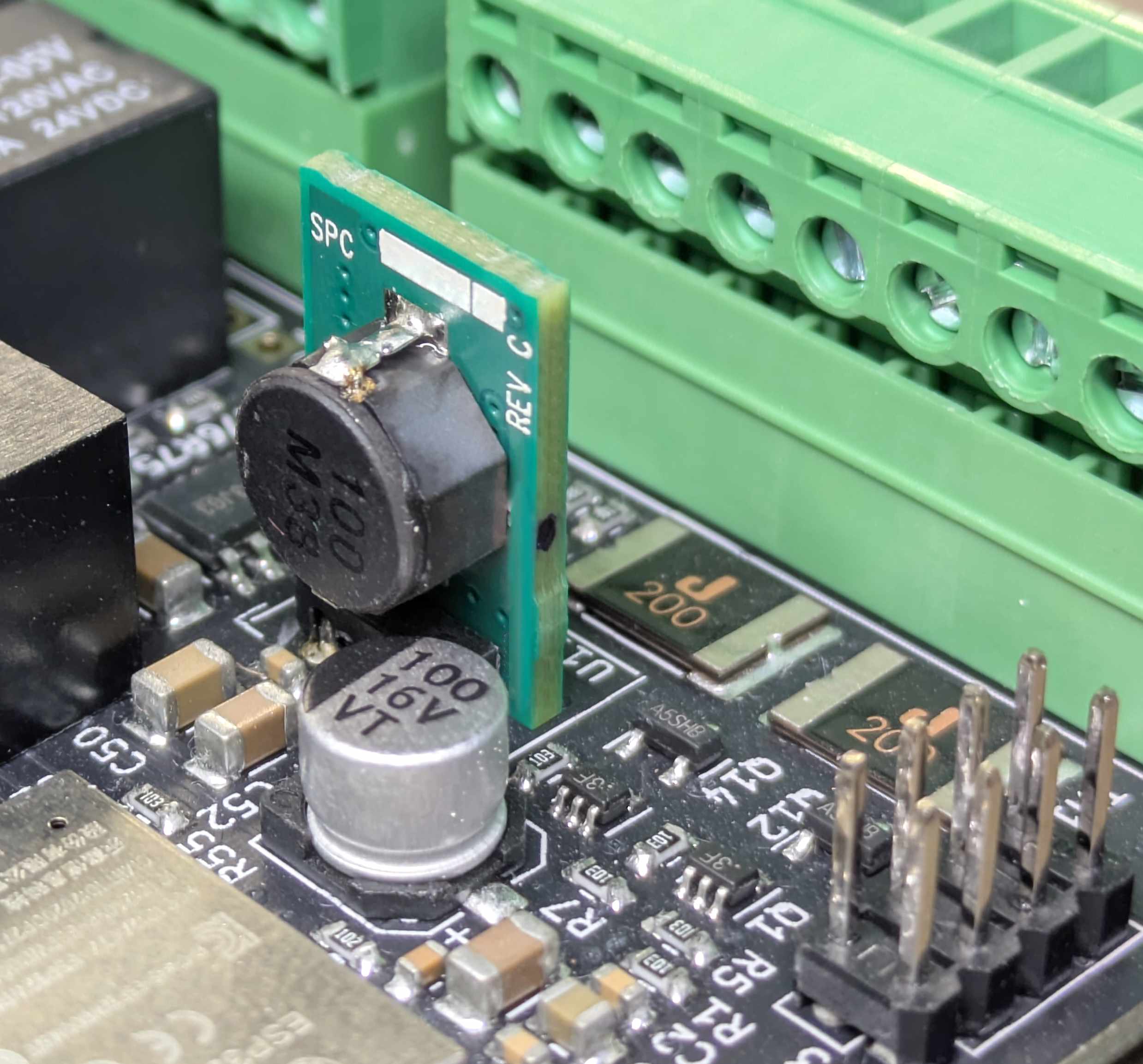
- For a supply above 5 V, fit a DC/DC converter at U19. The BSC Shop offers modules for input voltages up to 34 V, and separate 5 V supplies for redundancy or higher voltages. The square U19 pad is the converter's 5 V output: observe polarity. If using 5 V relays, use a converter rated >= 1 A, since U19 also powers them.
CAN/RS485
All interfaces are galvanically isolated and can connect directly, without adapters, to an RS485 BMS (Serial 0–10) or CAN inverter. Their voltage levels are standardised.
RS485 (BMS)
Some common BMS types connect directly through RJ45. Multiple devices may be connected by daisy chain where supported, or with the RJ45 Serial Distributor from the BSC Shop.
OneWire
Temperature sensors can connect without additional hardware. The required pull-up resistors are already on the BSC PCB.
Thermal Management
The top of the BSC PCB needs gentle airflow for cooling. Do not unnecessarily enclose or cover the board; provide continuous ventilation.
Digital Inputs
Technical Specification
- 4 inputs, 3–27 V DC.
- Galvanic isolation via optocouplers.
- Positive trigger edge (low to high); configurable software inversion.
Electrical Properties
Each input is isolated from the rest of the circuit. All four inputs share their own GND reference, exposed on the connector for an external supply or signal source. A separate 5 V connection is available for each input; these outputs share that GND and can directly supply push-buttons.
Software Inversion
Inverting the positive trigger edge makes a high-to-low transition trigger the input. This is useful for inverse logic or normally closed contacts.
Typical Applications
- Push-button: Connect 5 V to the button and its output to DI. Pressing it applies 5 V and triggers the input.
- Relay contact: Connect 5 V to one side of the contact and the other to DI. Closing the contact triggers it.
- External voltage, e.g. 24 V DC: Connect external GND to the GND pin and the signal directly to DI (3–27 V DC).
Relay Outputs
Overview
Six electromechanical outputs (Rel1–Rel6) provide external switching, controlled by configurable trigger events and timing options.
Hardware Specification
Maximum Switching Ratings
- DC: 24 V / 3 A
- AC: 120 V / 3 A
Available Contacts
Relays 1–3 expose NO (normally open), NC (normally closed) and COM (common). Relays 4–6 expose only NO and COM; their NC contacts are not brought out because of connector pin limitations.
Software Configuration
Configure each relay individually and assign one or more trigger events.
Configurable Parameters
- Pulse duration [ms]: Time the relay stays switched after an event, adjustable from 100–10000 ms. To keep it switched until the event ends, select Permanent, not Pulse.
- Delay after trigger event [s]: Delay between the event and switching, for sequential or staggered actions.
- Inversion: Reverses the switching logic: a trigger switches the relay off rather than on, or vice versa.
Trigger Events
Several configured events can be assigned to a relay at once. The relay activates if at least one assigned event occurs.
Application Examples
Load Shedding in Critical Battery Conditions
- Trigger: plausibility check (BMS data outside valid ranges).
- Delay: 0 s; pulse: 200 ms; inversion: yes.
- Use external DC contactors with a control input for high battery-pack currents, driven by the relay.
Periodic Fan Control
- Trigger: temperature threshold.
- Delay: 0 s; pulse: 10000 ms (maximum); inversion: no.
- For longer run-on times (e.g. 1 minute), use Permanent instead: the relay then stays switched until the trigger ends. Alternatively, implement the desired run-on behaviour with the alarm rule's temperature hysteresis.
Delayed Alarm Output
- Trigger: critical battery event.
- Delay: 10 s; pulse: 500 ms; inversion: no.
- In a critical event, first reduce inverter current demand through commands before triggering a hard disconnection using a contactor. This reduces hardware stress during faults.
Usage Notes
- PCB layout limits switching capacity. Use external contactors or solid-state relays for higher voltage or power.
- For inductive loads (motors, coils), use flyback diodes or snubbers.
- The NC contacts on relays 1–3 permit fail-safe arrangements for safety-critical applications.
- Pulse duration runs independently of the trigger event's duration.
Opening Solder Jumpers
Some factory-closed solder jumpers must be opened mechanically. A rotary tool can remove only the surface copper. Do not damage the internal copper layers.
Jumper Configuration
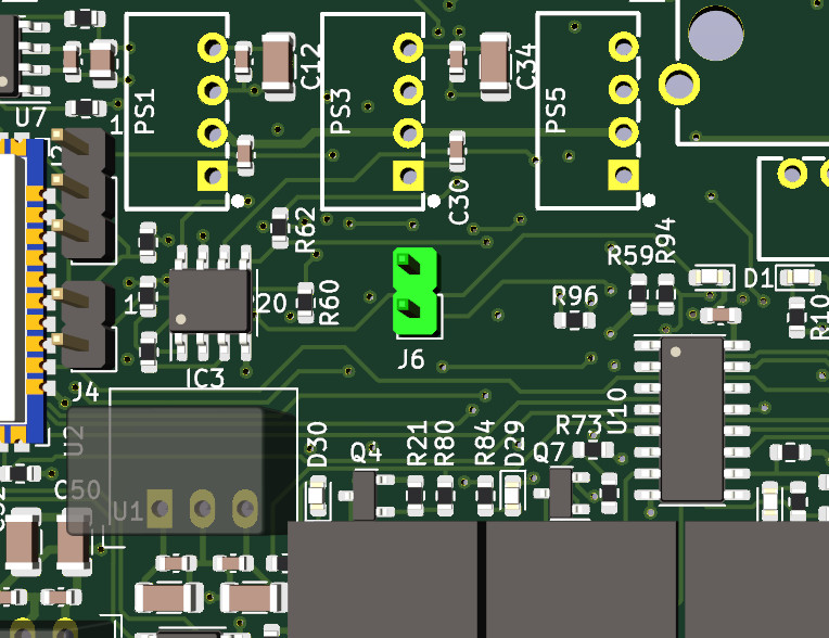
J6 for Normal Operation
Open J6 to program an unprogrammed board. Fit it for normal operation.
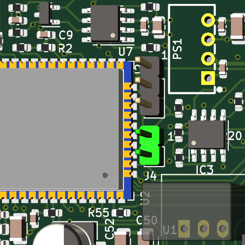
J4 for Programming
Fit J4 to program an unprogrammed board. Leave it open for normal operation.
Connecting Relay COM Contacts to Vin
Fit the corresponding jumpers to connect the relay common contacts to the board's Vin.
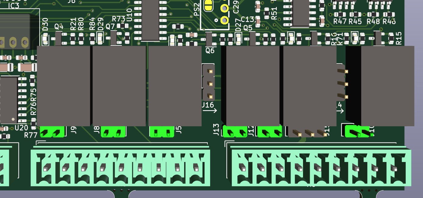
J14–J16: Enabling Outputs
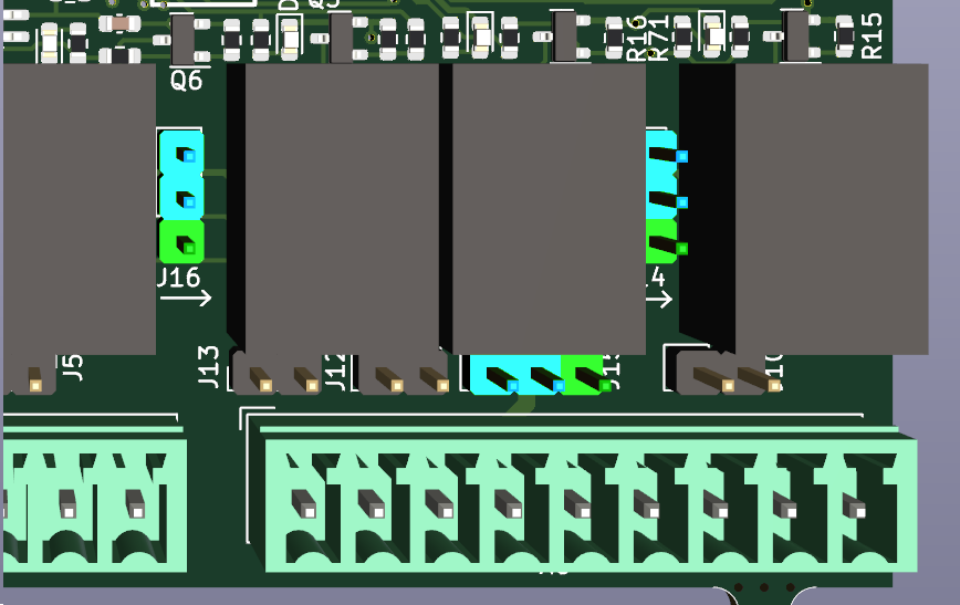
These relays have additional functions not currently supported by firmware. Set the jumpers to the positions marked blue.